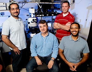
Illinois chip researchers. L-R: Graduate student Amir Arbabi, professor Gabriel Popescu, graduate student Chris Edwards, and professor Lynford Goddard (L. Brian Stauffer, University of Illinois)
Engineers at University of Illinois in Urbana created an etching and sculpting process for semiconductors using light that also monitors the etching process in real time. The team led by Illinois electrical and computer engineering professors Gabriel Popescu and Lynford Goddard published its findings today in the journal Light Science and Applications.
Chip makers need to precisely control the three dimensions of their components, which can affect performance, speed, error rate, and time to failure of the devices produced. Semiconductors are shaped by etching with chemicals, which can lead to errors, such as residual layers, that affect the further etching, as well as hamper device performance. As a result, time-consuming and costly processes are used to ensure precise etching, to within a few nanometers in some cases. (1 nanometer equals 1 billionth of a meter.)
The Illinois research team developed a process that simultaneously etches a semiconductor surface and monitors the etching in real time. The process uses a special type of optical microscope with two beams of light that very precisely measures the topography of the etching.
“Looking at the change in height, you figure out the etch rate,” says Goddard. “It allows us to figure out the etch rate both across time and across space, because we can determine the rate at every location within the semiconductor wafer that’s in our field of view.”
The dual-optical beam approach, say the researchers, offers advantages over conventional semiconductor etching. The new method is purely optical, thus making no contact with the semiconductor surface, which allows the researchers to monitor the whole wafer at once instead of point-by-point. In addition, the light catalyzes the etching process itself. The new method uses a projector to shine a grayscale image onto the sample being etched, which allows the researchers to quickly create complex patterns, and adjust them as needed.
Traditional chemical etching, in contrast, creates features in steps or plateaus. For curved surfaces or other shapes, semiconductor researchers use photochemical etching, where light shines though very expensive glass plates called masks that have distinct patterns of gray to let light through by degrees. A researcher must purchase or make a mask for each tweak of a pattern until the correct pattern of features is achieved.
The new method, say the Illinois researchers, is faster, lower in cost, and less noisy than the current methods of based on atomic force microscopy or scanning tunneling microscopy, which can only compare before and after measurements of the chips, not monitor them in real time. “You can use light to image the topography and you can use light to sculpture the topography,” says Popescu. “It could change the future of semiconductor etching.”

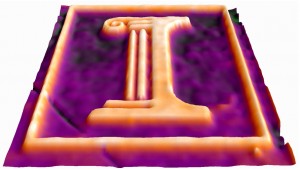
A three-dimensional image of an etched gallium-arsenide semiconductor. The height difference between the orange and purple regions is approximately 250 nanometers. Click on image for full-size display. (Chris Edwards, Amir Arbabi, Gabriel Popescu, and Lynford Goddard, University of Illinois)
Read more:
- Synthetic Nanomaterial Developed for Semiconductors
- Project to Study Light-Enabled Quantum Dot Circuits
- Nanotech Process Devised for Graphene Semiconductors
- NSF Grant to Fund R&D on Wireless Network Chip Connections
- Grant Funds Feasibility Study of Photonic Ethernet Chips
* * *

 RSS - Posts
You must be logged in to post a comment.