Researchers from the U.K., Netherlands, U.S., Russia, and Japan created a nanoscale electric power transformer from one-atom layers of graphene and other materials. The work led by Leonid Ponomarenko and Andre Geim at University of Manchester is described online in the journal Nature Physics (paid subscription required).
The process developed by Ponomarenko, Geim, and colleagues assembles individual atomic layers on top of each other in a desired sequence. In this case, the researchers used crystals, with a thickness of one atom, to build a multilayer stack that works as a nanoscale electric transformer — 1 nanometer equals 1 billionth of a meter.
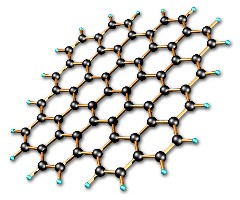
Graphene is closely related to graphite like that used in pencils, but consists of only a single atomic layer of carbon atoms. The material is very light, strong, chemically stable, and can conduct both heat and electricity. Geim and Manchester colleague Kostya Novoselov received the Nobel Prize in physics in 2010 for their work demonstrating the properties of graphene.
In the process used in this study, the researchers extracted individual atomic planes from bulk graphite and boron nitride with the same techniques for graphene that results in a single atomic layer of carbon. Then, they mechanically assembled the crystallite layers one-by-one, Lego-style, into a crystal with the desired sequence of planes to build the transformer.
The transformer has a one-atom-thick conductive plane of graphene with four atomic layers of boron nitride serving as an electrical insulator. In the transformer, electrons moving in one metallic layer pull electrons in the second metallic layer by using their local electric fields. For this device to work, the metallic layers need to be insulated electrically from each other but separated by no more than a few inter-atomic distances, thus the ratio of one conductive layer of graphene to four layers of the insulator boron nitride.
Geim noted that this process shows complex devices can be constructed plane by plane with atomic precision. “There is a whole library of atomically-thin materials,” says Geim. “By combining them, it is possible to create principally new materials that don’t exist in nature. This avenue promises to become even more exciting than graphene itself.”
Read more:
- Technique Devised for Controlling Graphene Nanopore Size
- BASF, Max Planck Institute Open Joint Carbon Materials Lab
- Nanotech Process Devised for Graphene Semiconductors
- Method Devised for Inexpensive Graphene Production
- Graphene Materials Faster, Cheaper at Cooling Electronics
- Manchester to Host U.K. Graphene Research Institute
* * *


 RSS - Posts
You must be logged in to post a comment.