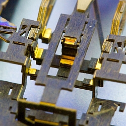
Engineers at Harvard University have developed a technology that makes possible the mass production of miniature electronic and robotic devices, using layering and folding processes similar to the Japanese paper-folding art of origami. Doctoral candidates Pratheev Sreetharan and Peter Whitney say their discovery is scheduled for publication in the March 2012 issue of the Journal of Micromechanics and Microengineering.
Sreetharan and Whitney developed these processes from their work on Harvard’s Micro Air Vehicles (Robobees) project to design miniature robotics patterned after bees in nature. Until they devised the new fabrication process, however, each device required assembly by hand, which not only took a long time, but also led to high error rates.
The new process enables Sreetharan and Whitney’s team to produce complex prototype devices, only 2.4 millimeters in height and about the size of a U.S. quarter. They use 18 layers of carbon fiber, a plastic film called Kapton, titanium, brass, ceramic, and adhesive sheets laminated together in a laser-cut design. The resulting structure has hinges that allow the three-dimensional units to assemble in one movement, like a pop-up book.
The team says dozens of these micro-robots can be fabricated at one time on a single sheet. In addition, the layering technique is based on manufacturing processes used today to make printed circuit boards, which means that the tools for creating large sheets of pop-up devices are currently available.
While the new techniques promise to streamline the manufacturing of micro devices, the design process is still a labor-intensive exercise. Standard computer-aided design (CAD) tools are made to design either flat, layered circuit boards, or 3D objects, but do not yet support devices that combine both.
Harvard’s technology transfer office has started the commercialization process for this work including the filing of patent applications.
The following video tells more about this project.
Read more: University Develops, Licenses Autonomous Robotics Technology
* * *


 RSS - Posts
[…] Mass Production Process Devised for Micro Robots, Devices […]